
~ High-accuracy packaging in panel level packaging ~
TOKYO, JP / ACCESS Newswire / March 27, 2025 / Toray Engineering Co., Ltd. (head office: Chuo-ku, Tokyo; CEO & COO: Takashi Iwade; hereinafter "Toray Engineering") has developed the UC5000, a high-accuracy semiconductor packaging equipment (bonder) for panel level packaging (hereinafter "PLP"); PLP is an advanced semiconductor packaging technology, for which there is growing demand particularly from AI servers. Sales of the UC5000 will commence in April 2025.
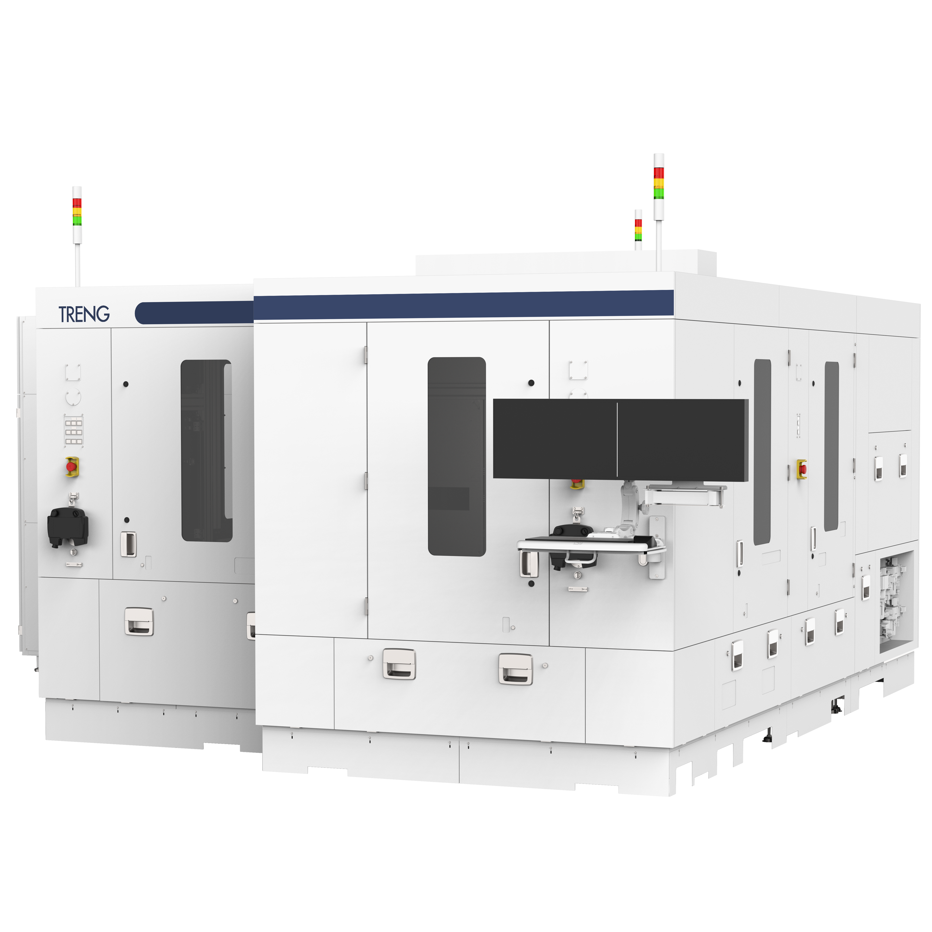
This system is capable of packaging chips with a high accuracy of ±0.8μm using thermal compression bonding (hereinafter "TCB") on 515mm × 510mm and 600mm × 600mm panels complying with the SEMI Standards. It can also carry out high-accuracy TCB packaging on glass panels, which is gaining attention as an alternative material to silicon, contributing to the manufacturing of next-generation semiconductor packaging.
Toray Engineering aims to supply the UC5000 to manufacturers of semiconductors, targeting 3 billion yen ($19.9 million USD) in orders in FY2025 and 10 billion yen ($66.4 million USD) in FY2030.
With the increasing performance of semiconductors, chiplets-a technology that packages several semiconductors chips into a single package, as represented by 2.5D packaging-is gaining attention. Wafer level packaging based on silicon wafers, such as those using interposers for high-speed transmission between semiconductor chips, was the mainstream for semiconductor packages comprising such chiplets. Going forward, with semiconductor packages becoming bigger due to increasing performance, PLP based on glass panels, which allow sizes larger than wafers and rectangular shapes, is gaining attention because wafers cannot grow larger in size and have poor manufacturing efficiency, having to cut rectangular shapes from round wafers.
However, compared to wafers, large glass panels warp significantly and are difficult to transfer, and require larger heaters to heat the panels. There were thus issues with heat control within system as well as difficulties in achieving high-accuracy packaging while taking into account the expansion and shrinking of materials due to heat.
The UC5000 achieves high-accuracy packaging of ±0.8μm on large panels and TCB through: a technology-used in TCB packaging equipment for small substrates, for which Toray Engineering has a mass production track record at least 100 units so far-that maintains accurate packaging, calibrating for impact from heat arising from high temperatures of 300℃ and higher during soldering; high-accuracy packaging technology and panel-warping correction transfer technology that were used in systems equipped with bridge chips for large panels, for which there is a mass production track record of at least 50 units; and a complete overhaul of the core control system for use in the UC5000. This system is also compatible with front-opening unified pods (FOUPs) for panels and tape frames that comply with SEMI Standards, which are starting to be adopted in the downstream processes of semiconductors, and its composition can also handle mass production at the latest plants.
Building on Toray's production technologies for advanced fiber materials, Toray Engineering has developed and refined microfabrication technologies for use in semiconductor packaging equipment, display production equipment, and a wide range of other equipment used in the field of electronics.
Besides the TRENG coater and large glass substrate inspection system, Toray Engineering will contribute to the further adoption of PLP by adding the UC5000 to the lineup for the field of advanced semiconductor packaging.
The details of the PLP-compatible bonder UC5000 are as follows.
Note
1. Product name: Panel level packaging-compatible bonder UC5000
2. Product features:
Compatible with panels complying with the SEMI Standards
(515mm × 510mm and 600mm × 600mm)Accuracy of 0.8μm using PLP and thermal compression bonding
Function for automatic calibration of accuracy deviation due to heat without affecting productivity
Capable of taking over functions of existing models through customization
3. Usage: Packaging of semiconductor chips for panel level packaging
4. Order goals:
3.0 billion yen in FY2025 ($19.4 million USD)
10.0 billion yen in FY2030 ($66.4 million USD)
About Toray Engineering
Toray Engineering is a global leader in innovative engineering technologies.
Established in 1960, we have been designing and providing plant construction and FA equipment, as well as state-of-the-art manufacturing facilities and equipment such as FPD/semiconductor production equipment, films, and display materials.
Under our business brand "TRENG", we contribute to society by creating new value and realizing solutions to bring about a sustainable society.
More information is available at www.toray-eng.com.
Media Contact
Amanda Steinberg
AH&M Inc.
Tel: +1 413-329-6887
asteinberg@ahminc.com
SOURCE: Toray Engineering Co., Ltd.
View the original press release on ACCESS Newswire